Light Rail Project Writeup, Part 1
Introduction
This project started from the simple desire for me to come up with my own concept for a hardware badge, akin to the ones you'd see at places like DefCon or SuperCon. If you are not aware, hardware badges are generally thematic, bespoke development boards with included hardware/peripherals that are easy to hack and modify. To me, the hardware badge is the perfect manifestation of the maker/hacker culture. They embody the curiosity to experiment and try new things, the desire to always be learning and improving, and most importantly the willingness and desire to share your project with the community so others can be inspired, learn from, and subsequently build upon your work. This last facet is the most important to me because it's the primary cog that drives the maker community. It is from this sense of sharing with community that really drove me really stop "lurking" and start putting my own projects out for others to see.
The process of getting my projects out into the public sphere at first was simply getting more organized and collecting my various existing project files into public Git repos. I definitely still have more work to do here! But in addition to sharing code and pictures, I also really value all of the project writeups I've read over the years from the multitude of other makers. I have really benefitted from those who have taken the time to both share their projects as well as composing their process into a helpful and informative writeup. So it is in that spirit that I decided to share my own experience developing this project with this writeup. Writing has never really been enjoyable for me, mostly because I feel so inefficient when I do. As a side benefit of pushing myself through this process, I am also hoping this writeup will serve as the basis for traning data for an LLM that could help me share even more in the future by writing in my own voice!
Design Inspiration And Concept
The overall design idea of Light Rail came together in my head unexpectedly, all at once. I was in bed, trying to wrangle my thoughts and fall asleep. I was struggling because my mental state was still buzzing with excitement after recently deciding to finally come up with an idea for my own hardware badge.
For months prior, I had been toying around with small projects, experimenting with different breakout boards for LED drivers, trying out all sorts of little ideas—fun animations for sensor data, a tunnel runner animation, a maze runner animation, a maze runner animation with enemy sentries, experimenting with RTOSes to see how many I2C displays I could smoothly animate, etc. Just scratching that itch for experimentation and the sake of trying things out. Then that night, I was looking at all of my flashy projects where I have them displayed in my office (a collection—not a hoard) when a thought hit me: "All of these projects are running your code, but none of them are your hardware!"
With that realization, I decided to think up and design my own unique take on a hardware badge. So there I was in bed, trying to sleep despite the random flurry of ideas that were popping into and out of my thoughts. I did eventually calm my mind enough to drift toward sleep. However, the calm in my head only lasted a few moments. The gears of my subconscious must have kept spinning because before I was able to fall asleep, in an instant, all of the chaotic swirling of all my earlier scattered thoughts came rushing back into my head. But then, surprisingly, the earlier chaos of ideas swiftly coalesced in my head with the precision, speed, and grace of a team of animal mechs assembling into Voltron.
It was a unique mental experience I won't soon forget! It's quite hard to describe, but I think I can manage to at least give a non-exhaustive list of the ideas/inspirations that ultimately coalesced into what is now Light Rail:
- trains, in general
- Lego trains (this is not my first train project! Also see my M5Cardputer firmware for controlling Lego trains and switches)
- my nephew who also loves trains
- Mini Metro, a game with trains
- PCB Convention Badges, especially Supercon 2022 badge
- TIGER Electronics handheld LCD games
- Adafruit LED backpacks, especially this one
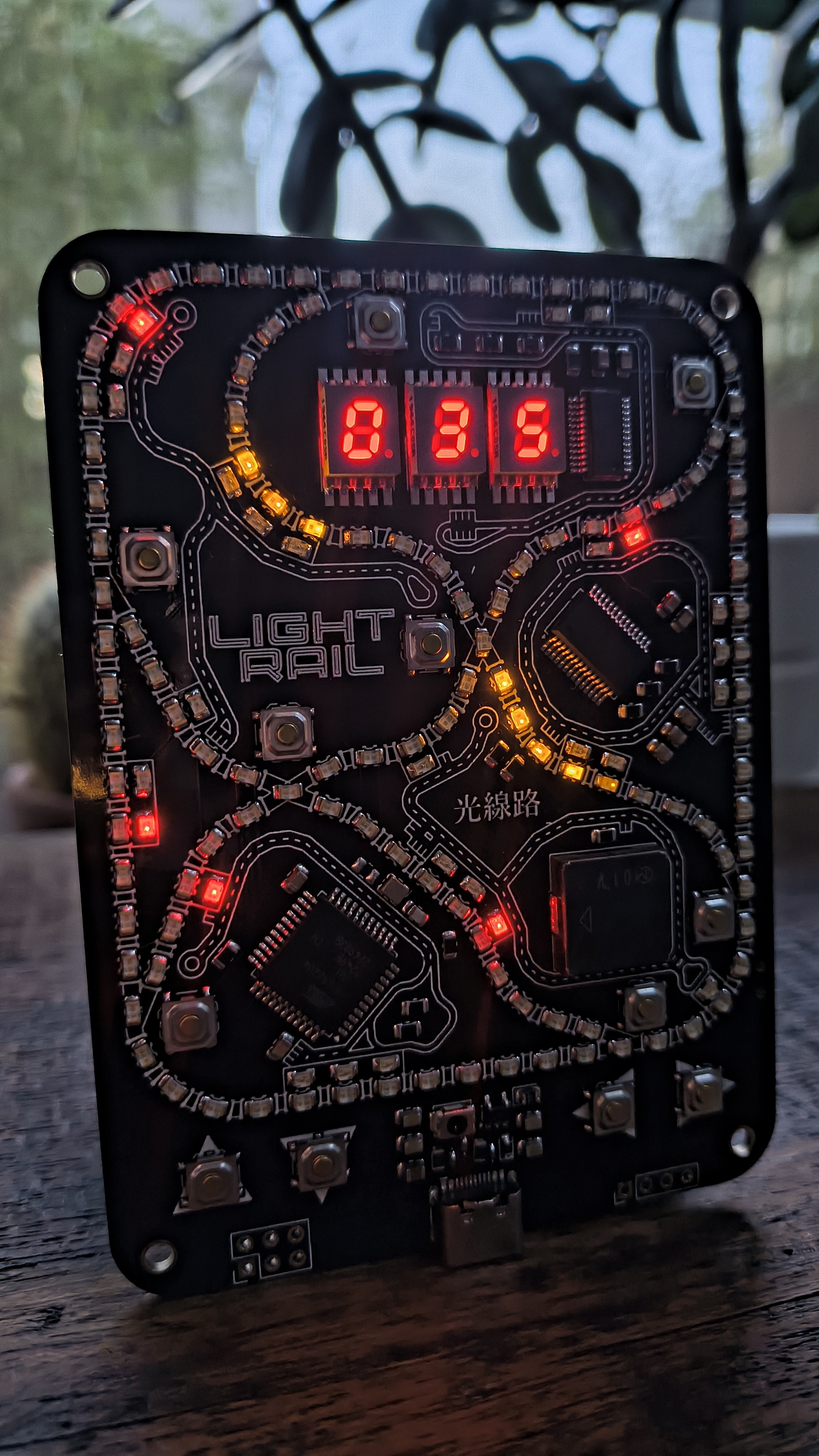
OK, so what was the actual idea? It was a train game. The tracks would be represented as lines of LEDs, with silkscreen graphics, and the trains themselves would be contiguous sequences of lit LEDs moving along those tracks—each LED representing a single car in the train. Arranged alongside the tracks would be other LEDs that would represent the platforms. When lit, a platform would indicate cargo ready for pickup, which a passing train could collect from an adjacent track and deliver to another platform elsewhere. The train's cargo could be visualized using bright LEDs for full cars and dim ones for empty cars. The track layout would include forks and crossings, each with a nearby push button to toggle or switch their state.
Later, I came up with the idea to also integrate the rest of the board's components into the visual theme—I added silkscreen roads and parking spaces around the various rectangluar ICs and platform LEDs to give the appearance that they were buildings on a map.
As for the gameplay itself, I never really prioritized it—even now, as I write this. It’s always been the least important part of the project for me. The main reason is simple: it's hard to know what will actually be fun without being able to playtest it. Instead, I focused on being thoughtful with the board design so that, once I had functional hardware in hand, the board itself would naturally inspire gameplay ideas. I wanted something flexible—something that would give me room to experiment and explore once I could see it in action. I just haven’t done that part yet. That’s for part two!
Hardware Design
Design Goals
As soon as the Light Rail idea hit me, I started right away. Like I mentioned earlier, I had been trying to fall asleep, but the moment the idea surfaced, I got up immediately and started chugging away at the initial schematic in KiCad. By the time I went back to bed, I had already finished the majority of what would become the final schematic!
Since that original burst of inspiration, the design hasn’t changed much. What did surprise me, though, was how the design process felt. From beginning to end, it was less about inventing things piece by piece and more about revealing something that was already in my head. That’s the best way I can describe it—it felt more like discovery than creation. Apparently, I had been designing it subconsciously for a while.
Even though I had a strong mental image from the start, I eventually found it incredibly valuable to distill all those swirling ideas into clear, articulated design goals. I didn’t do this early on. At first, I just held everything loosely in my head and followed the momentum of my excitement. But as I got further along—especially when I was trying to wrap things up—I started getting distracted by too many side ideas. Some of them were genuinely cool, but they strayed from the core concept.
My favorite example: I had recently picked up a few breakout boards for secure element chips and had been experimenting with them. That led to a new idea—what if I turned the project into a cutting-edge "cash-in-a-puzzle-box" gift? Like those plastic gift boxes where you need to solve a maze before you can get the money or card inside. The idea was that my board could function like a hardware wallet, using the secure element to store crypto keys. A parent could preload the wallet, lock it, and give it as a gift. The recipient would have to achieve some unlock condition—like a high score or solving a puzzle—before accessing the wallet. I still love this idea! But it wasn’t part of the original vision. And worse, it completely derailed my design progress for a few days until a few gentle epithets from my brother helped me realign.
So for me, the below design goals I outline were essential in trimming down the infinite possibility space into something more focused and manageable. At the core, it's just a mental trick I needed to use to stop my brain from being the enemy. The design goals helped me keep my overreaching curiousity tendencies in check and prioritize decisions that aligned with the original vision—not just flashy add-ons or nice-to-haves.
No Matrix.
The board would not use an LED matrix—or anything resembling a traditional rectilinear layout. This was my very first design goal, set in stone before anything else. It was actually my next thought after deciding to come up with a design at all. Why? Because it would act as a forcing function, pushing me to come up with something unique. LED matrices are everywhere. I wanted to avoid the cookie-cutter pixel grid and make something that didn’t look like anyone else’s board.
The 2022 Supercon Badge was a big inspiration here—even though it does use a matrix for some LEDs. What I admired about it was how the LEDs represented meaningful state in a simulated 4-bit CPU, rather than just acting as generic pixels. That concept stuck with me.
Aesthetics > Gameplay
One natural consequence of avoiding a matrix was that the layout of tracks and platforms on the board would be fixed. That meant less potential for gameplay depth or variability. So I made a conscious decision early on to prioritize the board’s aesthetic appeal over its gameplay mechanics.
In other words, I chose form over function—and I leaned into that choice when I was doubting myself. Even with the limitations of a “fixed” board, I remembered how much fun I had with Tiger handheld games as a kid. Those were incredibly limited, using static LCD displays with static graphics, and yet still managed to be enjoyable and have foundational memories from them. So I felt confident that I could conceive of some enjoyable gameplay ideas despite the constraints.
Without this design goal clearly in mind, I probably would’ve struggled with the lack of gameplay flexibility. But every time that doubt crept in, I reminded myself that this tradeoff was intentional—and core to the vision.
Learning, Not Earning
As much as I’ve always wanted to design my own hardware badge, I’ve also been drawn to the idea of creating products to sell as a fun hobby—like so many do on Tindie, Etsy, or eBay. But I also know myself: I have a tendency to get ahead of things and try to do too much at once. I realized early on that I needed to give myself the space to learn—not just chase the idea of building something sellable.
So while this project might eventually become a step toward hobbyist product design, I made sure it was not the focus. I made a deliberate choice to prioritize learning and experience over productization. (Refer back to the hardware wallet tangent that nearly derailed the design!) If I hadn’t made that design choice, my attention would’ve been split, and I doubt I would’ve finished the project with the same clarity—or satisfaction.
Choosing the Hardware
I leaned heavily on my recent experience from smaller projects where I played around with different dev boards and Stemma QT/Qwiic breakouts, testing various types of LED matrices and arrangements. That hands-on exploration really helped me develop a sense for what I liked—and what I didn’t.
One of the earliest decisions I made was to avoid Neopixels. From my previous experiments, I found them finnicky to work with at low brightness levels, and they tend to draw more baseline current than standard LEDs. They’re also more expensive and I was worried about not being able to repair them by hand. But the biggest reason just comes down to visual aethetics--they look harsh (at least to a dark-mode diehard like me)! I like them most tolerable behind diffusers, which certainly was not something i was going to consider for my project.
IS31FL3731 + LEDs: These ended up being a straightforward design choice for me. I had a good experience working with it in the Adafruit LED backpack, where I found it very easy to do smooth animations with full individial PWM control for each LED. I considered similar chips like the IS31FL3741 that could control more LEDs, but thought that 144 LEDs was a good number. Red and yellow were the natural choices for two basic warm colors with maximum contrast.
Kingbright 7 Segments + AS1115: I chose the Kingbrights because they are smol and fit well in the board aesthetic of "components are buildings". There's no specific design decision with the AS1115, I just found a IC driver for seven segments that communicated over I2C and had an inline package that fit well.
ATMega32u4: I chose this primarily because it's a commonly used AVR chip in other designs and it has built-in USB. I had actually never used this chip before, but have experience with other AVR chips, so the USB capability felt like a useful bonus for debugging or future features. Plus, it would make it way easier to let friends or family reprogram the boards—I could just give them a script and skip the need for a separate USB-to-serial chip. But it's pretty expensive for what it is, ~$5/chip, so I definitely wouldn't have chosen this without the learning design goal.
Power Circuitry: I pieced this together mostly by reviewing schematics from other dev boards and similar projects. I did some fairly hand-wavy math for my expected maximum current draw for my board, and made sure the LDO regulator could source well above that.
Buzzer: I used the same piezo buzzer that comes with the ACK1 coding kit hardware. The biggest factor in choosing it was how well it fit into both an empty space on the board as well into the design concept of "chips are buildings". It’s relatively large for a piezo, but simple enough to drive directly from a microcontroller pin.
Layout
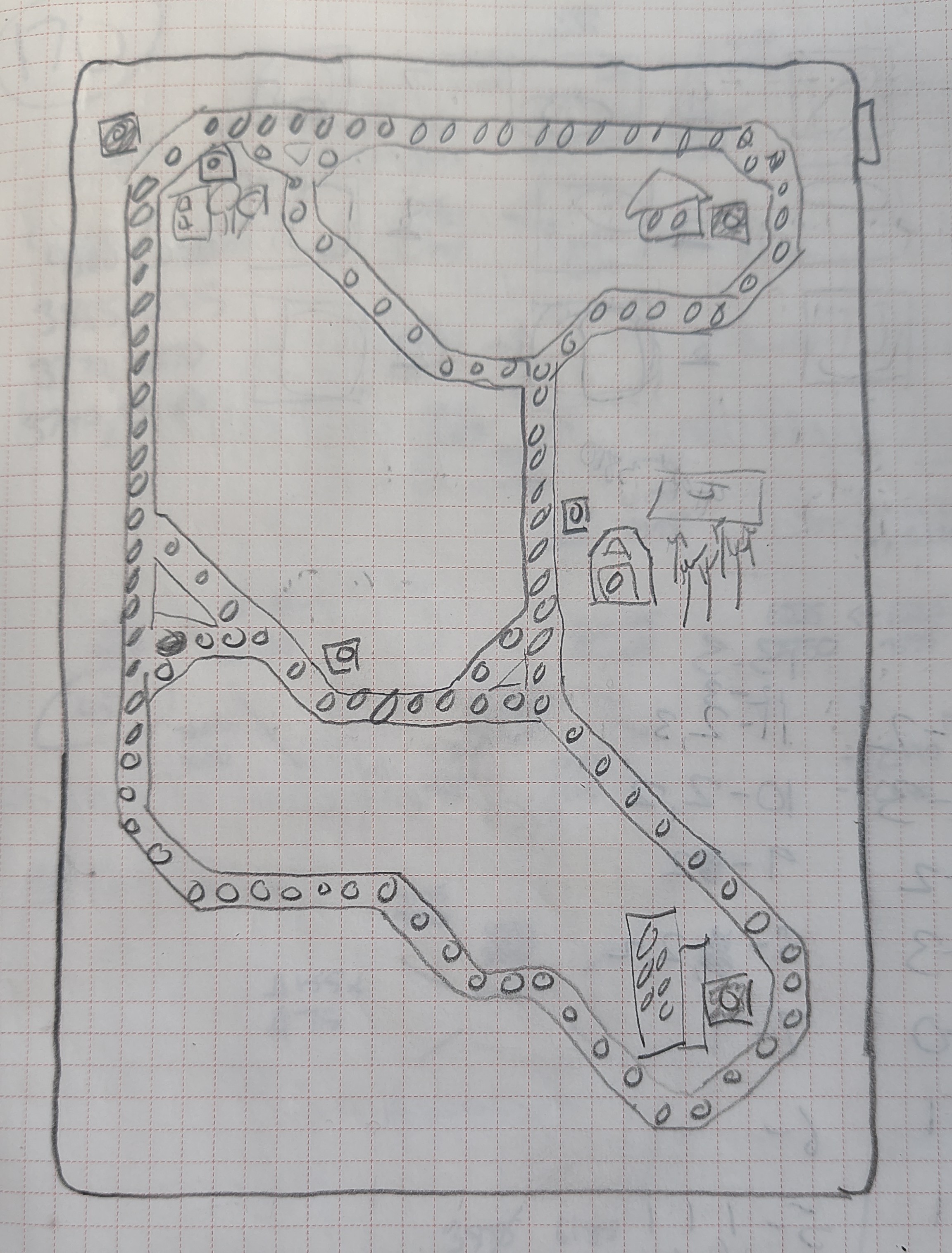
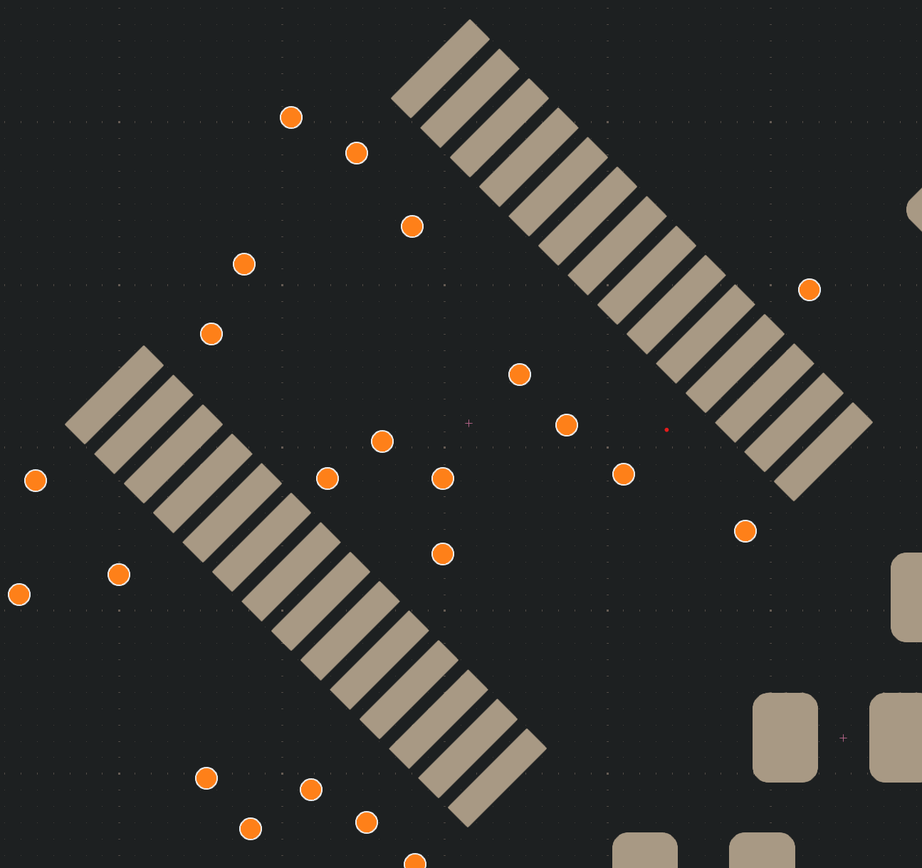
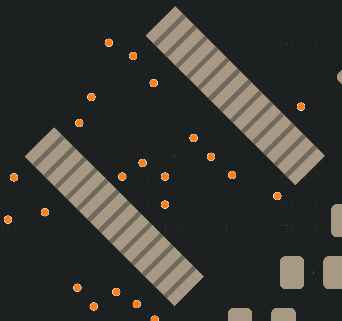
Layout was definitely where I spent the bulk of my time. I started by roughly laying out the LEDs to form the outer loop of the track. Then, I drew the board's outline/edge cuts. KiCad’s raytracer was super helpful here to give me a good visual sense of the LED spacing and adjust the overall proportion/margins. I also found some similar sized flat objects that were roughly the same size as the board's external dimensions and held them up to my monitor to get another perspective for how the board might look and feel in-hand. With the outer loop in place, I used my original notebook sketch as a rough guide to lay out the inner tracks and forks. Once that basic track layout was drafted, I was happy to see I still had plenty of LEDs left over for the platforms, which I added in groups to each section of track.
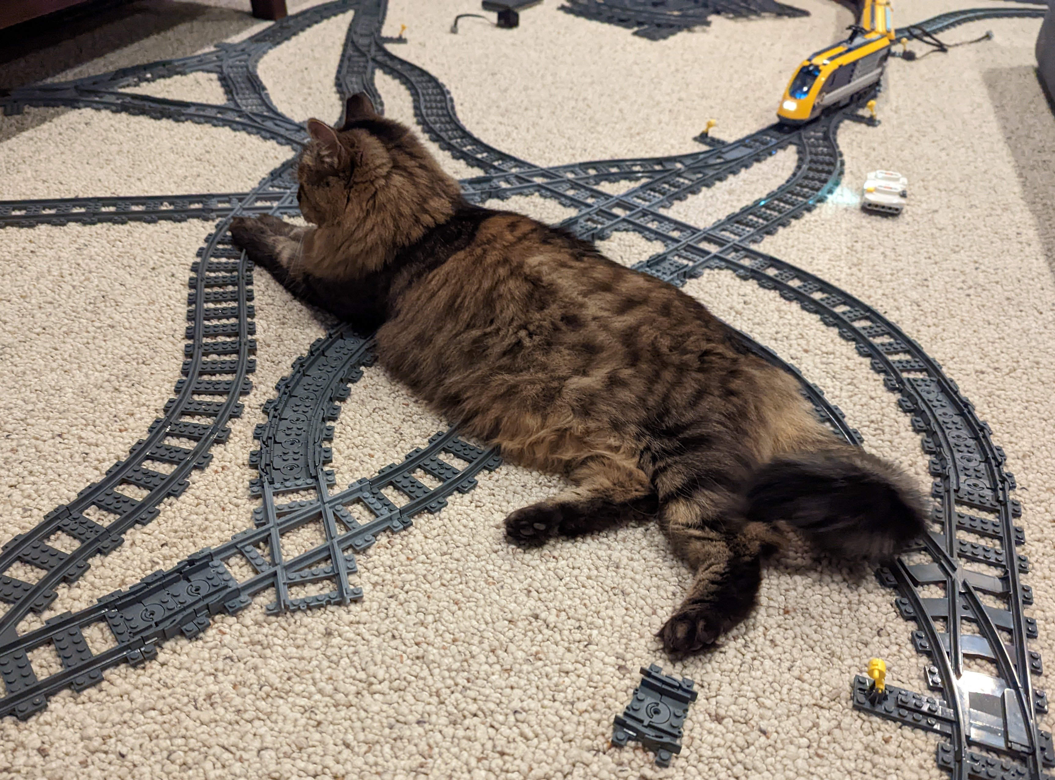
From there, I leaned on my experience designing wildly impractical Lego train track layouts (see image) to tweak a few key parameters:
- Length of track sections between forks/crosses
- Direction of forks along a given track
- Platform distribution in each track section, relative to length of section
Once the track layout felt right, I moved onto the rest of the components. I put the ATMega near the bottom to keep it close to the power circuit and USB connector. The IS31FL3731 went right in the middle of the board to minimize trace length to the LEDs. At the top, I placed the Kingbright seven-segment displays and AS1115—these would serve as the game status/score display. Buttons were placed next to each fork and cross to function as toggles, and I added four control buttons at the bottom for gameplay input.
Before I started routing traces, I was pretty sure I’d need a 4-layer board due to trace complexity of routing to all of the LEDs. So, I began by defining the two inner layers as power and ground fills. This effectively created a large parallel-plate capacitor out of the board itself. This would help, at least in theory, with voltage stability across the board, where it would complement the existing ceramic capacitors on the board. (Mental note: at some point I'd like to run the number to get an estimate of the actual capacitance based on board area, copper thickness, and layer spacing—just to see how much it actually contributes.)
The IS31FL3731 drives its 144 LEDs as two separate 9×8 matrices, so I made sure to group the LEDs accordingly during layout. But after routing the top section, I wasn’t happy with the result. The trace paths felt unbalanced, and while PWM operates in the relatively chill kHz range, I still didn’t want to deal with potential weirdness from trace capacitance variations. So I reworked the layout, treating it more like a logic puzzle where the goal was to minimize overall trace length/count by repositioning LEDs to better group common anodes and cathodes.
I tried an autorouter partway through the process and left it on overnight. That's about all I have to say about the autorouter.
Meanwhile, KiCad had its own set of small annoyances. For instance, I tried saving a few traces by connecting ground to just one pad on a button footprint (since the others were internally connected), but KiCad wasn't having it. As far as I can tell, there's no clean way to define implicit connections within a footprint that’ll keep the design rule checker happy—at least not without resorting to something that feels even more hacky than just editing the footprint itself to satisfy the DRC.
Once layout was done, I spent way too much time drawing silkscreen roads and tiny parking spots. For how small they are, I obsessed a bit too much over getting consistent widths and spacing. But I thought turned out great, my artistic skill notwithstanding, so... only minor regrets there. When I showed my mockups to my family, I immediately got comments about how the components looked like buildings. Instant validation.
Ordering, Manufacturing, Assembly
Order Preparation
Before this project, I had only done one other project that used PCBs of my own design—my Stemmett project—so I had pretty limited experience with the various options for PCB manufacturing and assembly. Luckily, early in the design process, PCBWay reached out to me about a potential collaboration. Since I hadn’t tried their services before, it made the choice of manufacturer really easy! Looking back, I genuinely don’t have any real issues worth mentioning—just good things to say about the whole experience.
Getting started with the ordering process was super smooth, thanks to PCBWay’s KiCad integration. They have a plugin you can install directly from KiCad’s plugin manager, which adds a menu option that opens your browser and pre-fills their ordering form with your Gerbers. That alone saved me a bunch of time and clicks throughout my design iterations compared to my last project.
I also decided early on to go with full assembly for the boards. This freed me up during the design process to focus more on aesthetics instead of worrying about the complexity or hand-assembly viability of each part. Plus, I knew going through the assembly experience would be valuable for future projects. While I don’t have other services to compare it to, my experience with PCBWay’s assembly was smooth and pretty painless overall.
The most time-consuming part of the assembly order process was preparing the Bill of Materials (BoM). I did this manually using PCBWay’s BoM sample template as a guide, which was really helpful. KiCad has some ability to generate BoMs, but I decided—at least for my first time—to raw dog it. It was a crash course in datasheet spelunking: making sure I had the exact manufacturer part numbers, learning the myriad SMD package types (and all the weird naming overlaps), and double-checking all the tiny details. I ended up relying heavily on Digikey’s product pages for this, since I found their descriptions and data formatting to be much more consistent than Mouser’s.
Ordering and Assembly With PCBWay
Once I finished the BoM, I could submit the order. Unfortunately, I realized soon after hitting submit that I had uploaded the wrong version of the BoM. But to my relief, I was able to get in touch with customer service almost immediately through a live chat window on the order page—ostensibly human as well (though you can never be sure now). They addressed my concerns quickly and let me know I could just email my assigned rep directly with the updated file.
After submitting the order, I spent the next few days working out a few kinks in my layout through some back-and-forth with the review team. The main issue was that the minimum solder mask bridge width for the black solder mask was slightly less forgiving than the standard green. That meant a couple of the ICs on the board had pin gaps too narrow for the solder mask to "bridge" between them. The fix was simple: just remove the solder mask between the pins. I was initially concerned this might increase the risk of solder bridging or shorts, but after a bit of reading, I found that it’s actually not that uncommon—especially when the chips aren’t being hand-soldered. Since I wasn’t planning to assemble the boards myself, I felt comfortable with the change.
The reason it took a few rounds to get right, though, was mostly due to my struggles with getting KiCad to actually apply the fix. On my first attempt, I found the “Solder mask minimum web width” setting under the solder mask/paste options in the layout editor. The tooltip said, “Min. dist between two pad areas. Two pads nearer this area will be merged during plotting.” That sounded exactly like what I needed. The default was 0, so I changed it to PCBWay’s requirement for the black solder mask (0.22mm), shot back the Gerbers, and called it a day—without actually checking if it had worked. (It didn’t do anything). For the second attempt, I spent way too long fiddling with settings trying to get KiCad to just fill in the gaps between pads like I expected. Eventually I gave up and manually drew solder mask exclusion zones around the pads—it took about two minutes as opposed to maybe an hour or two struggling to figure out KiCad settings. I sent the updated files back to PCBWay, only to realize later I’d completely forgotten to apply the same fix to the other IC that had the same issue. So: one last revision and my board layout finally passed review.
After resolving the board layout issue, the next step was getting everything squared away for assembly. This was my first time going through an assembly process, so I was prepared for unforeseen issues. But overall, the experience with PCBWay ended up being much smoother than I anticipated. As part of the initial order prep, I sent them a couple of near-final BoMs, and they sent back an updated version with quotes for the parts. I had opted for PCBWay’s turnkey assembly, where they source all the components themselves. Since it was my first time and I had no strong expectations, so I was pleasantly surprised to see that most of their component quotes were either cheaper than or on par with what I’d pay ordering directly from Mouser or DigiKey. The bigger surprise, though, was just how fast the total cost of components per board added up! My first instinct was to dive headfirst into cost-optimization mode (the ATmega was immediately on the chopping block), but I reeled myself back in by remembering my design goal: learning, not earning. Phew.
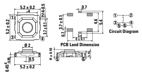
That said, the process wasn’t without hiccups. There was a roughly two-week delay where I was unknowingly holding things up. PCBWay had sent some engineering questions via email, but I completely missed them. I had been checking my order daily on their website, where there is a tab for engineering questions, and had not seen any indication. This is definitely my biggest piece of feedback for PCBway if they are reading! Please make sure engineering questions sent via email also show up in the website’s order dashboard! The engineering questions themselves were straightforward. They needed an extra reference image for the LED orientation and clarification that components I had marked "DNA" in the BoM did not need any solder mask (which was frivolous given the DNA marker, right?). A couple of assembly-related issues also cropped up. One was entirely my fault: I made the mistake of swapping out the reset switch in the schematic and BoM, but I had forgotten to also update the footprint so it wouldn't work on the boards that had already been manufactured at that point. Fortunately, the fix was easy! I found a switch that matched the footprint and PCBWay was able to sourced the new part, for the same price, and it only delayed the assembly process one day!
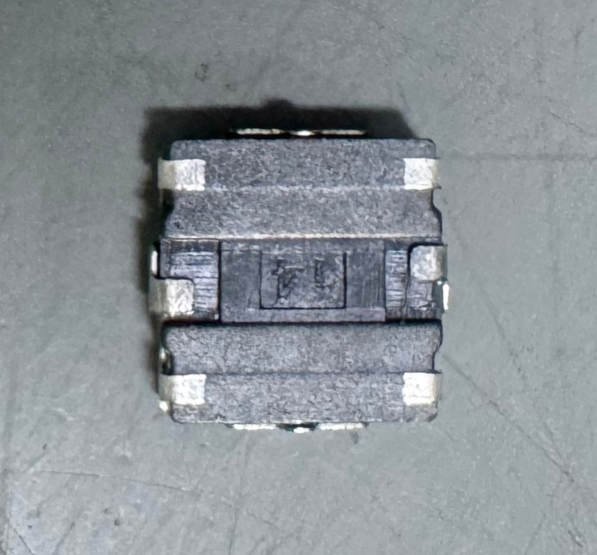
The other issue was that the footprints of all the other buttons on the board did not match the footprint of the actual buttons, oof. But in this case, it was entirely out of my purview or control because the buttons didn’t match their own datasheet. PCBWay also pointed this out with a screenshot of the datasheet and photo of the buttons. Thankfully, the mismatch only affected the positioning of the ground pins, so the buttons were still solderable and fully functional.
About a week after clearing up the engineering questions, I got an email with annotated photos of an assembled board. PCBWay wanted me to confirm the LED and seven-segment display orientations. The LEDs were good, but I spotted that the seven-segments were upside down. After responding, I got another email with new photos the very next day showing the board with the corrections, and I gave the thumbs-up to assemble the rest. Four days later, the boards shipped! When they arrived, they were nearly perfect! The only asssembly issue was that component C1 was missing on every board. Ironically, however, due to my own design issue, the component C1 ended up being unnecessary.
Design Issues
Clock Source
I didn’t select a clock source until fairly late in the design process. I had placed a placeholder symbol and footprint in the schematic and only swapped in a CMOS oscillator near the end, when I was focused on wrapping up the layout. Unfortunately, I only glanced at the pin mapping table in the datasheet—and skipped the rest. That oversight caused the ATmega chips to be completely non-functional when the boards arrived. I had ordered the SKU with default fuses set for an external clock, but due to my mistake, the MCU had no stable clock source. Worse, I couldn’t even get an ISP programmer to recongize the chip so I could read and update the fuses! Thankfully, after a few hours of debugging, I was able to fully diagnose and resolve the issue.
After digging back into the datasheets for the ATmega and the oscillator, and doing a little research into the differences between passive crystals (XTAL) and active oscillators (XO), the issue, and my mistake, become known. When the ATmega fuses are configured for a crystal oscillator, both the XTAL1 and XTAL2 pins are used as part of the whole oscillator circuit. That means XTAL2 is not stable during normal operation. But in my schematic, when I had replaced the crystal with an active oscillator, I had left XTAL2 connected to the oscillator’s tri-state pin, where I unknowly made the assumption that the pin functionality was the same. When I read the oscillator datasheet again, this time thoroughly, I realized that I had left the oscillator's tri-state (minor gripe that it didn't say enable pin) pin on a non-stable input--an invalid state for the oscillator to be in.
My first workaround was a literal glob of solder between the XO's enable pin and the adjacent VCC pin. That kept the oscillator always on, and finally let me communicate with the ATmega with an ISP programmer. Later, I built a pogo pin jig that I could press down carefully on the board to temporarily short those same pins during programming. That allowed me to update the fuses to use an external oscillator (not a crystal), which disables the internal oscillator circuit and frees up XTAL2 as a GPIO. Once the fuses were updated, XTAL2, as a GPIO, then defaulted to a floating/high-impedance state. Since I had carefully read the oscillator spec, I knew that leaving the enable pin floating was a valid "enable" state, and the oscillator could function with no solder or jigs required.
After that change, I plugged the board into my computer via USB—and boom, the stock DFU bootloader showed up in Windows Device Manager! Good feels.
USB/USB Bootloader issue
Once I had the DFU bootloader showing up over USB, I wanted to try using the Caterina bootloader. This is the "standard" USB bootloader found on many Arduino-family ATmega32u4-based boards like the Leonardo, Adafruit Feather 32u4, or SparkFun Pro Micro. Unfortunately, after flashing th Caterina bootloader, things stopped progressing. No variation I tried worked—each time I plugged the board in, Windows reported it as a non-functional USB device.
It was frustrating: the stock DFU bootloader showed up fine, so why not Caterina? After a bunch of head-scratching, I decided to re-flash the stock DFU bootloader to sanity-check my hardware and try flashing via DFU. Weirdly, I had to dig up the original DFU bootloader binary from some GitHub repo—I couldn’t find any official download from Microchip. I supposed I could have also read the flash data from one of the boards that still had it. Thankfully for my sanity, reflashing the DFU bootloader worked. The boards showed up again in Device Manager, and I was subsequently able to easily flash a firmware hex using dfu-programmer and see my code running on the boards!
At that point, I decided to shelve the Caterina investigation and move on. There didn’t seem to be much benefit in spending more time chasing down the issue when I already had a working toolchain for flashing code. My current theory is that the Caterina bootloader negotiates a faster USB bus speed than the DFU bootloader and is hitting some kind of timing issue—possibly due to clock instability or something subtle in my board layout. It could also be a USB signal integrity problem—maybe the impedance isn’t quite right, and tweaking the resistor values on D+/D− could help. Since I don’t know much about USB internals yet, and digging further would require a decent amount of ramp-up time, I was fine leaving it alone for now.
Conclusion and Next Steps
All in all, I’m really happy with how this project turned out. I learned a ton and got exactly the kind of hands-on experience I was hoping for—especially when it came to debugging and coming up with workarounds and fixes for design issues. I’m thankful that the problems I ran into weren’t insurmountable. Some of that was luck, sure, but a lot of it came down to taking my time, reviewing the design carefully, and coming back to it repeatedly with fresh eyes instead of rushing to place the order.
The mistakes I did make mostly revealed gaps in my review process. For example, I read the datasheets for the driver ICs over and over, yet somehow never gave the two-page oscillator datasheet a proper read. On the other hand, I could’ve pored over the button datasheet countless times and still not predicted that the components wouldn’t match spec (who does that!?!?). That contrast really drove home an important point: you can’t plan for everything—but that doesn’t let you off the hook for due diligence. The key is focusing your energy on the parts of the process you can control, and being ready to adapt when the unexpected inevitably shows up.
That wraps up the first half of the write-up! I made an interesting decision midway through this project: after submitting the order and while production was underway, I decided to implement all of the firmware in Rust. I’d “learned” Rust a few times before, but I didn’t speak it—because I’d never actually used it to build anything, so none of it really stuck. Well, I can say now that I’m a convert. Learning Rust—even if I never use it again—has made me a better C++ programmer, and a better programmer in general. The second half of this write-up will be about that journey.